
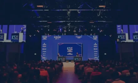


Silicon Box opens a $2B Semiconductor packaging facility in Singapore
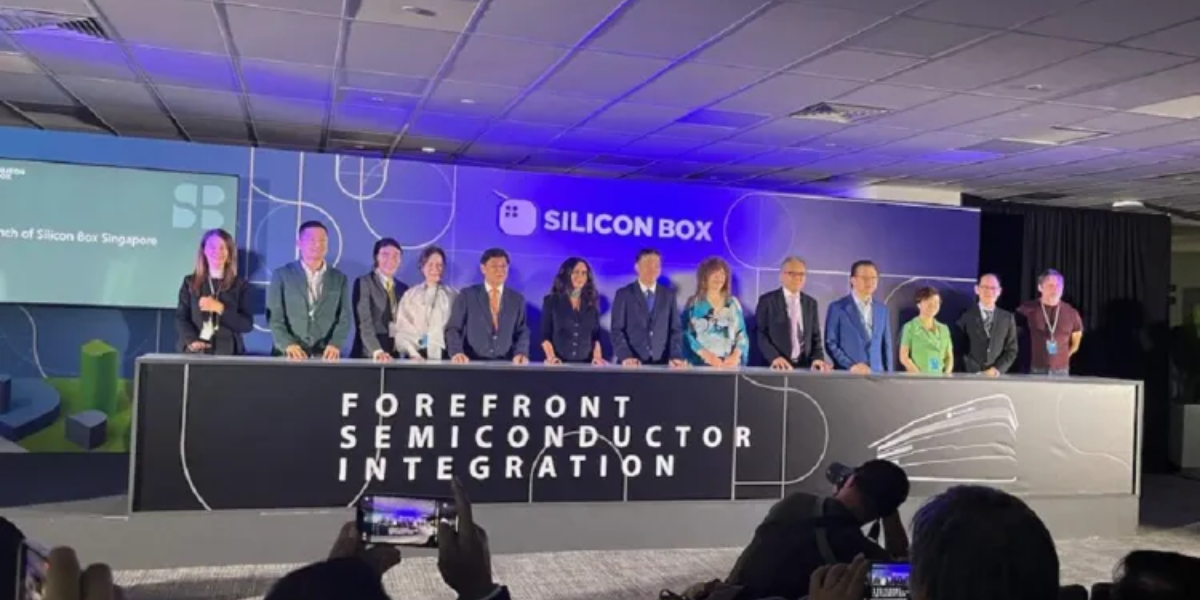
Silicon Box has inaugurated an advanced semiconductor packaging fab worth $2B in Singapore. The facility is located in the Tampines Water Fab Park. It aspires to revolutionize chip manufacturing, foster local capabilities, and elevate Singapore’s status as a prominent global hub for semiconductor production.
Moreover, the Singapore Economic Development Board (EDB) has actively supported this endeavor. According to the founders Dai, Sutardja, and Han, their company has identified an opportunity in chip manufacturing and design advancements called “Chiplets,” a term coined by AMD’s CTO, Mark Papermaster. According to Sutardja, this technology was first proposed for smartphones. As he said; “I was proposing this technology in the ISSCC talk in 2015 for the purpose of building your smartphones, your laptops, everything”.
The Rise Of Chiplets:
In response to the slowdown of Moore’s Law, which predicted chip advancements every few years, the chip industry has embraced the concept of chiplets. Chiplets involve connecting chips and chiplets with numerous metal connectors. This approach allows for continued chip design progress despite miniaturization challenges, with circuitry now just a few atoms thick and circuit widths around 5 nanometers. Companies like AMD have endorsed chiplets for both CPUs and GPUs. They have recognized that traditional manufacturing improvements that fueled the industry for years are diminishing. As a result, chiplets are becoming an increasingly vital strategy to maintain chip performance and cost-effectiveness in light of the limitations of miniaturization.
The chiplet approach has yielded impressive results, including 54% higher performance per watt, 18% higher frequency, 2.7 times peak bandwidth at 61 teraflops, and two times instructions per clock compared to the previous generation. According to Sutardja, the concept of chiplets allows chip designers to optimize performance and power consumption in large chip designs while keeping costs reasonable. Silicon Box’s proprietary fabrication method sets a new standard for design flexibility and electrical performance at a lower cost, vital in semiconductor design cycles. This agility in design cycles enables the industry to harness the chiplet concept, doubling computing performance and significantly reducing costs for graphical processors, high-performance computing chips, and mobile processors.
Silicon Box’s Solution:
Siliconbox is a company with 70 employees and is rapidly expanding. They have developed a proprietary fabrication method that offers exceptional design flexibility and electrical performance at a lower cost. To achieve high-speed and low-latency AI technology, Silicon Box creates large chips resembling panels containing multiple chiplets for efficient connections. Their target is to build 9,000 panels weekly. While this factory is not as expensive to build as a wafer fabrication factory costing billions of dollars, it still requires sophisticated technology, including a clean room and expensive packaging equipment. Silicon Box acknowledges the demand for AI applications exceeds their factory’s current capacity, indicating their determination to scale up and meet the industry’s needs. Silicon Box has established global partnerships with industry leaders to provide semiconductor solutions to drive next-generation applications.


